Cybermanufacturing Wide Bandgap Semiconductor Devices
You can design the highest performance, smallest form factor semiconductor device in the world—but if it can’t be reliably manufactured, its impact will be limited. Reliable, high-quality manufacturing is particularly important as the industry moves to newer materials that can surpass the physical limits of silicon. ECE’s Yuhao Zhang is collaborating with Hiu Yung Wong and his team at San Jose State University to help wide bandgap semiconductors achieve their promise with a new manufacturing process—aided by machine learning.
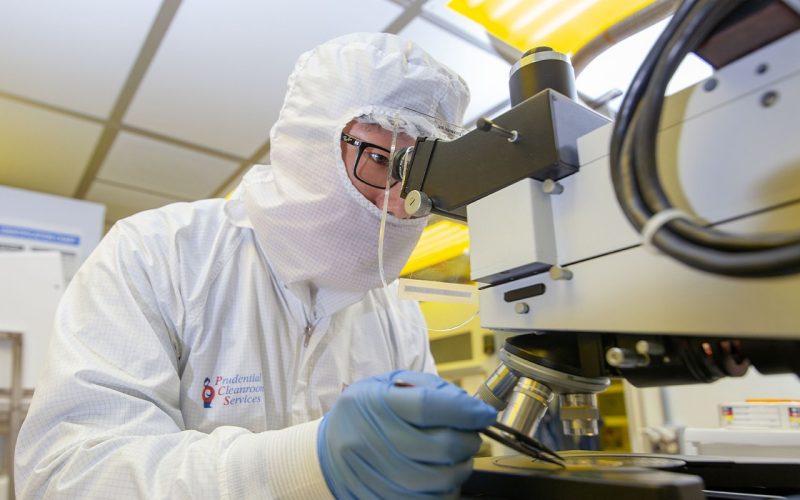
Typically, semiconductor devices, like computer chips, are manufactured on 6–8-inch wafers, which house thousands of devices that are later separated. Fabrication involves many steps, each of which must be nearly perfect to attain the high yield necessary for efficient manufacturing. This works very well for traditional semiconductor devices, like those based on silicon, explains Zhang, who is an assistant professor at the Center for Power Electronics Systems (CPES). However, newer materials like gallium nitride (GaN) and silicon carbide (SiC) can introduce more deformities and variability during manufacturing.
Machine learning for higher yield
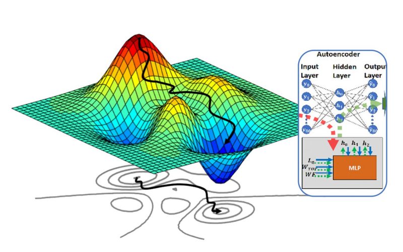
Zhang and Wong’s solution uses machine learning to compensate for the variability introduced in each step for each device, leading to a high yield even for the newest semiconductor devices.
Because there could be hundreds of parameters that affect these devices during manufacturing, the machine-learning algorithms can help determine the correlations and what changes to make at each manufacturing step to compensate for any variability.
For example, one area of a wafer might have slightly higher resistivity, Zhang explains. “An algorithm would automatically enlarge the area of the devices fabricated on that area so they can meet the specification.”
To train the algorithm, the team is collecting data from both experiments and simulations. The experimental data requires the team to fabricate devices and characterize the wafer at every step. However, “this data alone is not enough to train a highly accurate machine learning algorithm,” explains Zhang. They will augment the experimental data with Technology Computer-Aided Design (TCAD) simulations. “These simulations might take into account a thousand parameters that can impact the device performance,” says Zhang. “As we iterate and change these parameters, we will collect more data for the machine learning algorithm.”
Initially, the team will be testing their ideas using GaN power rectifiers, which require only six fabrication steps. “We want to identify any knowledge gaps,” notes Zhang, before moving to more complicated devices.
In addition to the manufacturing challenges, the team is employing broad knowledge to prove that this new process is feasible—including microelectronics, physics, materials science, statistics, and machine learning.
“We are exploring a completely new way of manufacturing semiconductor devices,” says Zhang. “If successful, this will have a very high impact.”
The result if Zhang and Wong’s team is successful? Billions of dollars in savings, reduced waste, and faster research and development of new devices.
RECENT RESEARCH BREAKTRHOUGH
Another of Zhang’s projects—a medium-voltage Gallium nitride high-electron mobility transistor (HEMT) that operates in enhancement mode above 10 kV—was recently highlighted by Nature Electronics as a research breakthrough from the 2021 IEEE International Electron Devices Meeting, which took place in December 2021.