Packaging for power: CPES Power Electronics Integrated Packaging Lab

The promise of power electronics to improve the efficiency and reliability of our nation’s electrical grid depends in large part on packaging the components to maximize performance and minimize cost. New materials, new algorithms, and innovative architectures cannot succeed if they are too expensive and cumbersome to implement.
The solution, according to Christina DiMarino, assistant director of the Center for Power Electronics Systems (CPES), requires not only packaging innovations, but also engineers and scientists who are skilled in the highly niched specialty of power electronics packaging. CPES, the leading research center of its kind, is answering that need with a new innovative power electronics packaging lab in Northern Virginia.

Meeting the packaging challenge
The CPES integrated packaging lab provides students and researchers with the resources, support, and the inspiration they need to find new ways to improve power electronics packaging.
Integrated into the grid, power electronics can actively control the power flow and add new functionalities like bidirectional power flow and islanding, a technique for isolating a fault. Reducing the size of power electronics can cut back on the amount of material used as well as installation and maintenance costs. But then the challenge is packaging.
Bad packaging can cause a fault in the system. If the package fails, the semiconductor device could overheat, resulting in a short-circuit or open-circuit failure.
“When you have high voltage over a small distance and high electric fields, you need to develop strategies for grading those fields and selecting appropriate materials,” explained DiMarino, who is an ECE assistant professor. “That’s what we're doing here in the packaging lab.”
At the cutting edge
Along with materials, algorithms, and innovative architectures, packaging and integration is a critical component that CPES targets on its mission to advance technology and prepare the workforce of the future.
Located in the National Capital Region at the Virginia Tech Research Center-Arlington, the new lab was built thanks to $143,000 in donations from 33 donors to the ECE General Fund. The lab strengthens relationships with industry partners and government agencies. Students forge career opportunities and working professionals in the greater Washington D.C. area have access to graduate studies in power electronics systems.
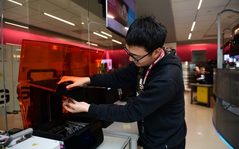
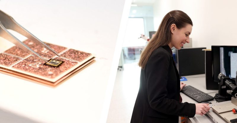
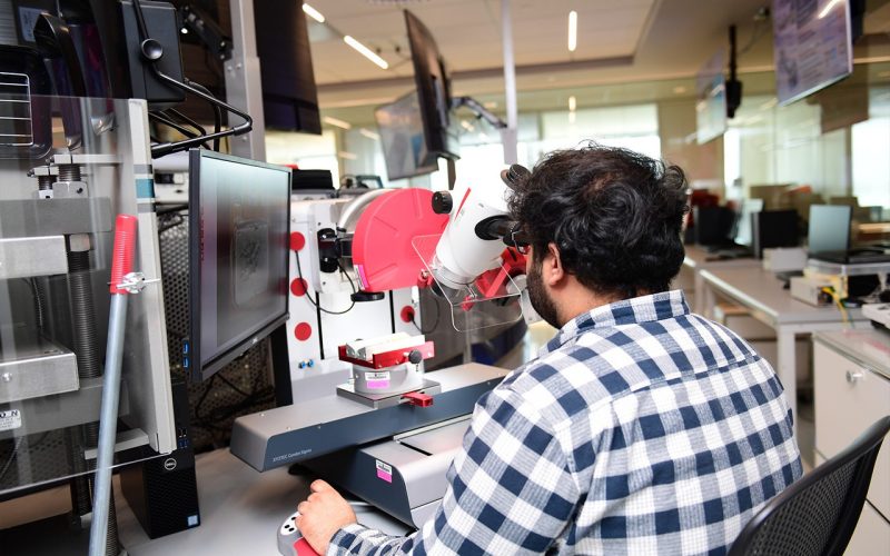
The lab is equipped to process materials, evaluate electrical characteristics and performance, analyze thermal performance and thermo-mechanical reliability, laser cut, etch, and 3D print, among other capabilities, said DiMarino.
Normally, the manufacturers install and calibrate new equipment, but during the COVID-19 pandemic, those tasks have fallen to lab faculty members and students.
“It’s been time consuming and challenging, but I think we all better understand the equipment—especially that new thermal analyzer,” said DiMarino. “Now all my students are itching to use it to test their packages.”

A snapshot of the integrated packaging lab’s new equipment
Programmable hot plates set the appropriate temperature profiles and can be used for solder reflow processes or silver centering, which is an alternative to solder that enables higher thermal conductivity, improved reliability, and better high temperature operation.
The hydraulic hot press enables pressure-assisted centering for bonding larger areas.
The wire bonder is fairly traditional for power electronics packaging, but the CPES lab will soon be receiving a die bonder for more advanced interconnect bonding for power electronics packaging like flip-chip packaging—where you flip the chip upside-down to achieve a shorter interconnect—and the ability to bond discrete interconnects onto the die directly. The latter yields greater current capability and double-sided cooling for more power output than traditional wire bonding.
A bond tester tests the quality of the bonds, measuring how much force it takes to shear or pull off a bonded component.
Thermal cycling chambers subject assembled packages to thermo-mechanical stress, and accelerates failure. Then the researchers can perform detailed failure analysis to understand exactly how the packaging failed.
A thermal analyzer allows researchers to gauge thermal resistance and heat flow. The machine also allows for active power cycling, which uses the semiconductor as the heat-generating component, as it would be in the actual application, creating different failure mechanisms. It also allows researchers to measure individual thermal resistances for each the package components.


